
This procedure applies to twin LNBs of the Golden Media type. DC supply and the intermediate frequency are routed through one F connector, while the LO reference is fed in through the second connector. The modification is outlined in the schematic below.

Procedure
- Open the LNB and remove the silicone sealant.
- Power the LNB with 12 V and probe the crystal oscillator with a scope – it can also sit on the opposite side of the PCB. Find the pin that shows the highest level.
- Remove the oscillator and the capacitors (Cs) at that pin, using a hot air gun or two soldering irons.
- At the LO connector, remove the printed inductor (PCB-L) and the capacitor to the mixer.
- Freely position the resistors (Rs) and capacitors (Cs) from the LO connector to the free oscillator pad. Different LNB versions need different routings. Use tape to isolate PCB tracks.
- At the intermediate frequency connector, remove the printed inductor (PCB-L) and replace it with a 2.2–4.7 µH ferrite bead. Make sure the ferrite bead’s resonance frequency is far away from 400–800 MHz.
- Test with an external power supply and LO. Current consumption should be 100–120 mA.
Photos
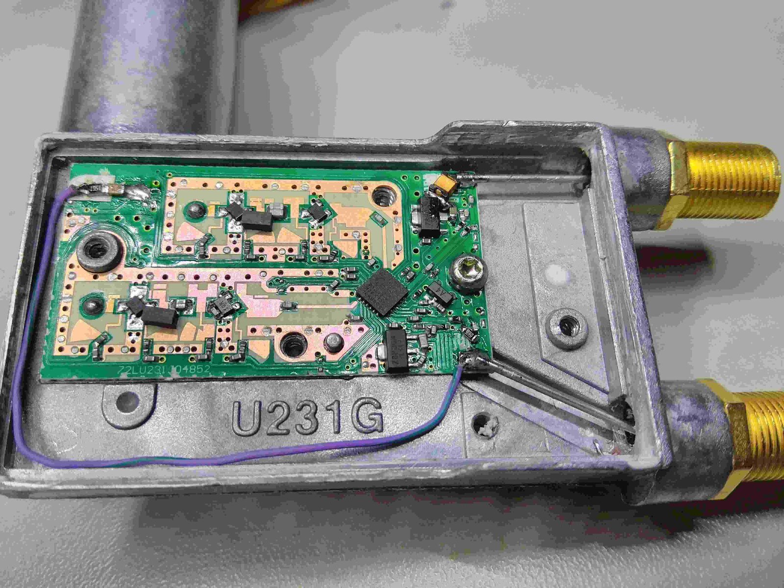
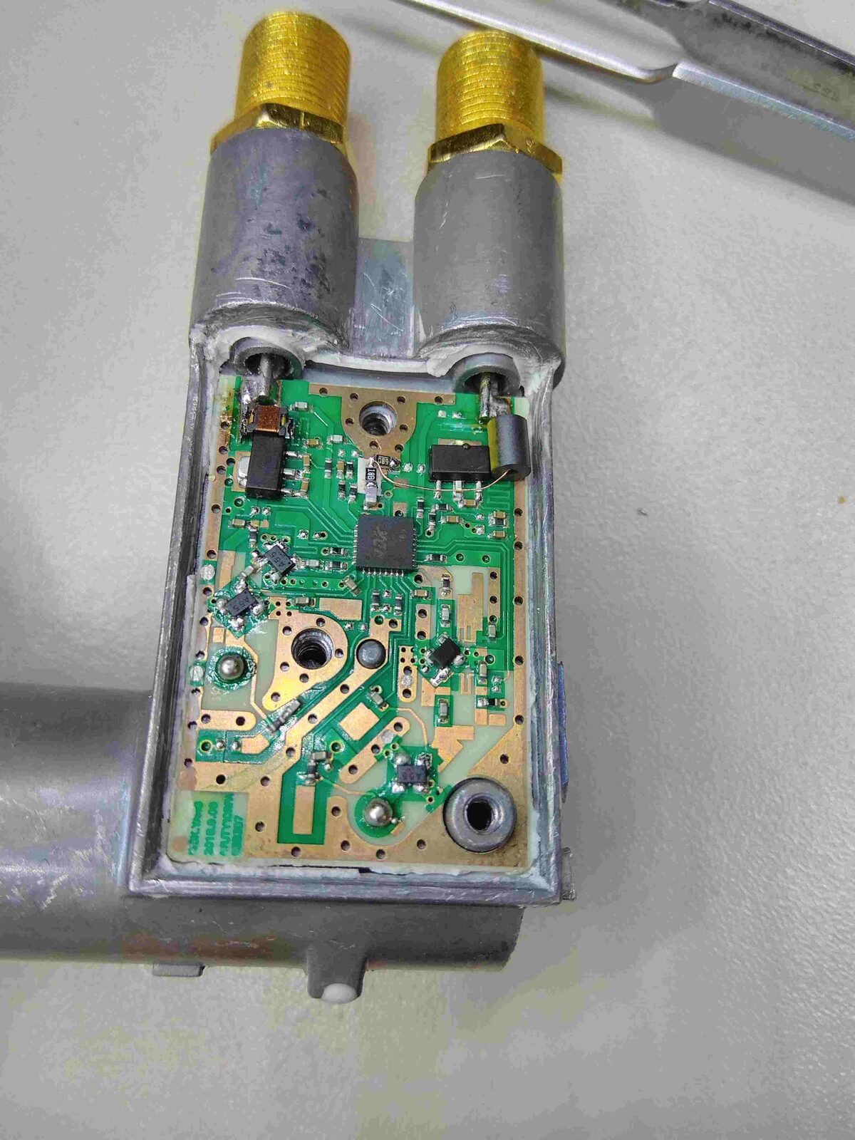
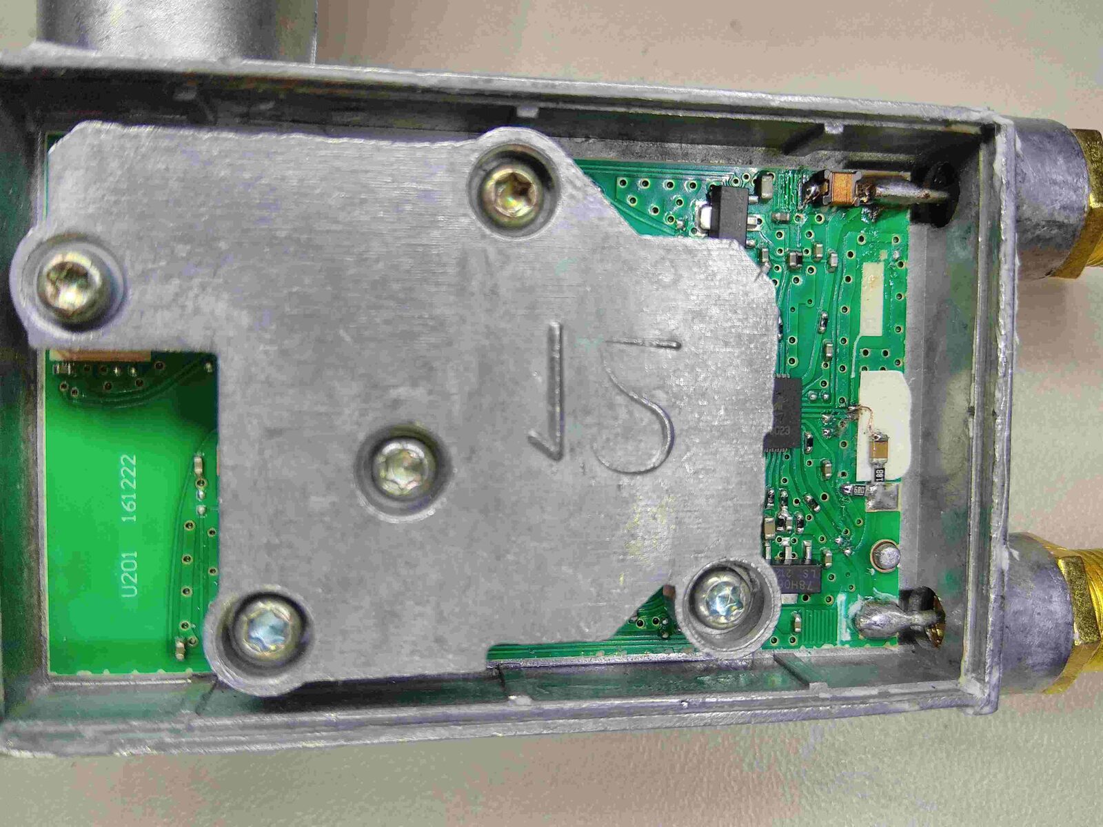

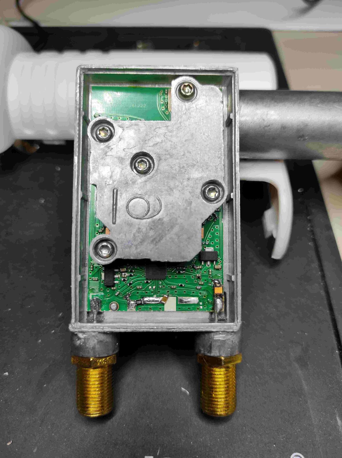
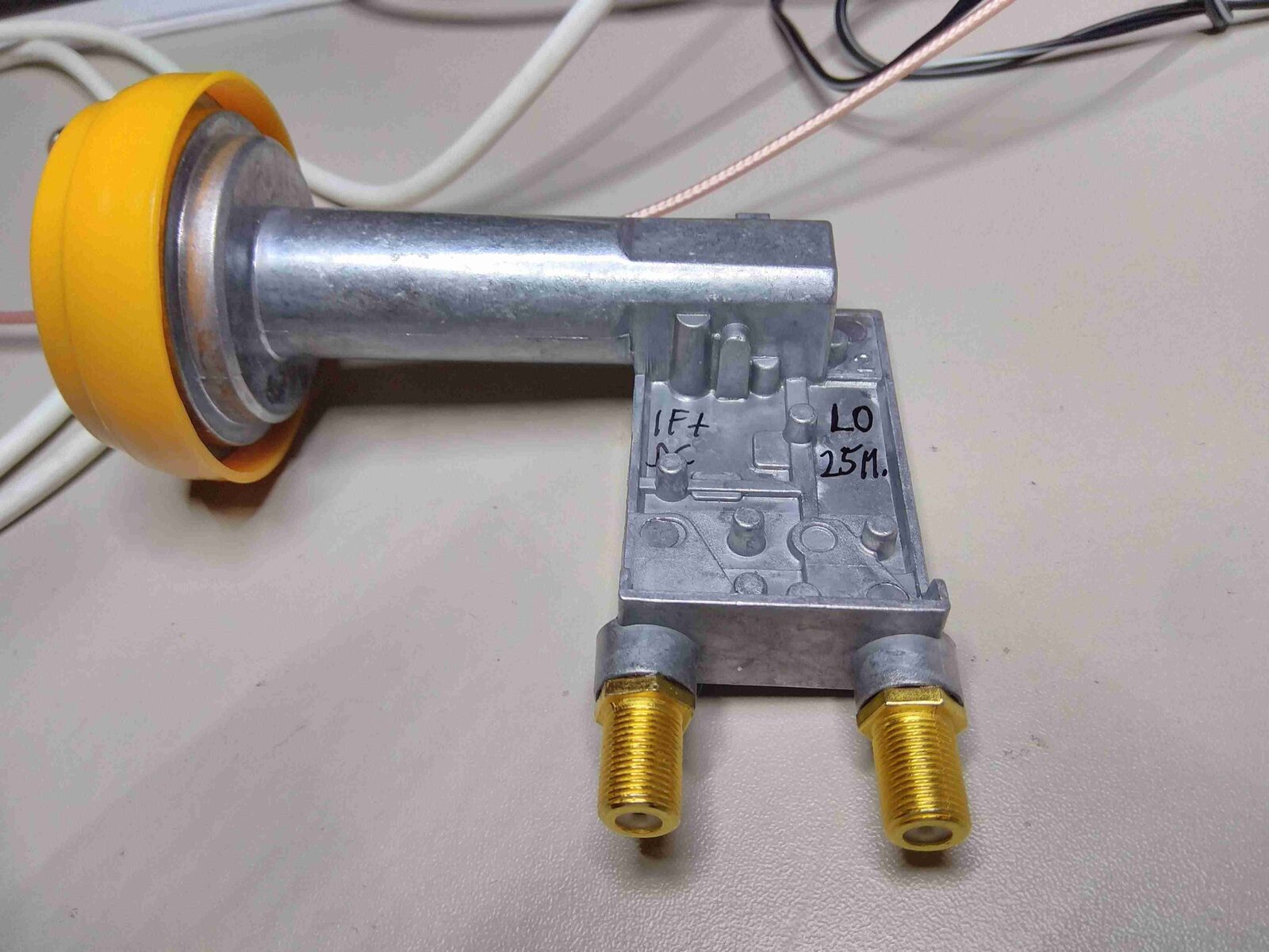
Courtesy of DL9SBY